
Tektronix Engineering Power Supply
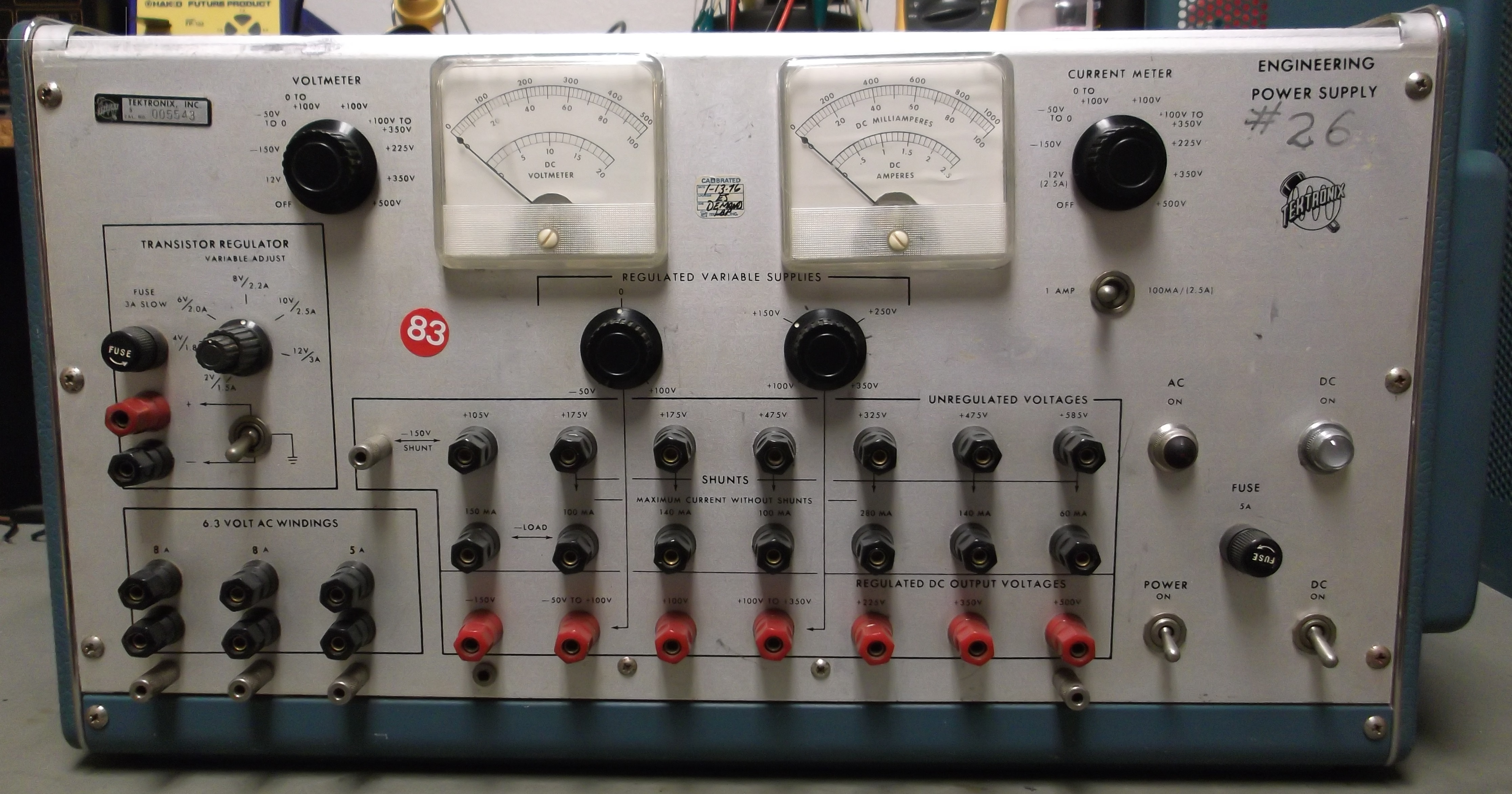
The Tektronix Engineering Power Supply, #26. These gems were not made for sale, but for internal engineering use at Tektronix here in the Portland area. My example, Mr. 26, is in very good condition and fully operational. It was not when found, the worst failure being in the low voltage “Transistor Regulator” portion. This section was dead. A few tube and capacitor changes were all that was required to bring up everything else. Repair of the Transistor Regulator, which is merely a variable regulated low voltage supply, was a challenge. Several components were burned beyond recognition, and the circuit present did not match the schematic! A little reverse engineering, guesswork, and component testing got it working well enough. Here’s some pictures of the unit while I get to work on entering schematics and an operation guide. I know there are a few folks out there with these who do not know how to use all of the features. This will be my gift to you!
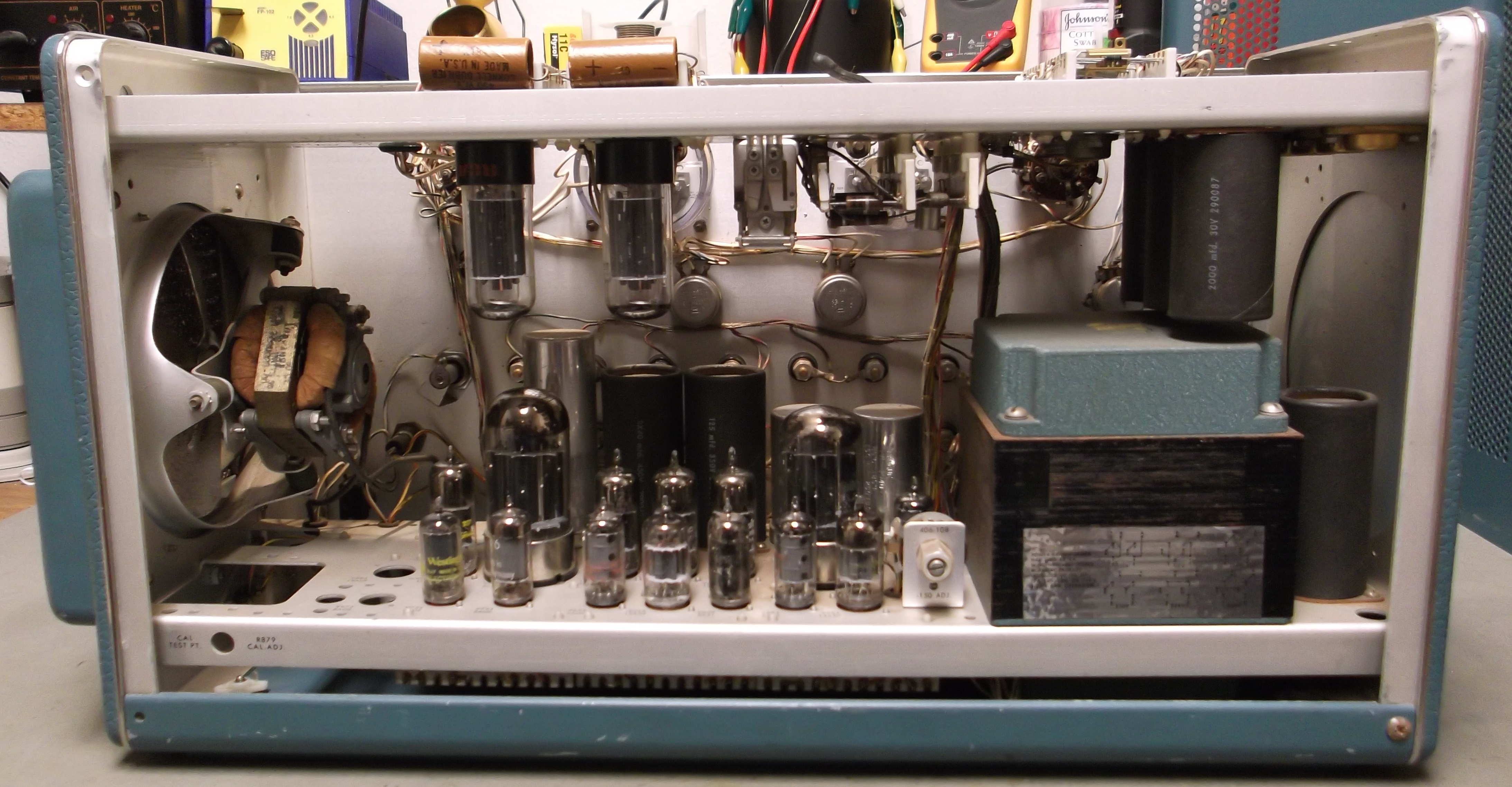
Here’s the inside view. All cleaned up, it only required new 12B4 and 6080 pass tubes, and of course the low voltage regulator repaired.

A close-up of the inside for your inspection! Note that there were unused tube socket mounting holes which have type identifiers. Either the design was changed, or the chassis plate is from another product. Most of the circuit here is copied from the model 585 oscilloscope, so it may be native to that. Other regulator sections present here, like the variable supplies using 6CK4 as pass tubes, seem to be unique to this design.

Here’s the first page of the schematic redrawn. This part of the circuit is nearly identical to the power supply in the models 545 and 585 oscilloscope. There are some vague component designators and some unreadable items so there will be errors. Use at your own risk!

Here’s page two, detailing the -150V regulator/reference, and the +100V supplies. The formulae to calculate shunt values are given with examples. These were worked back into equations from the original nomographs. If you’re interested in good old-fashioned nomographs, contact me and I’ll redraw those as part of this series!
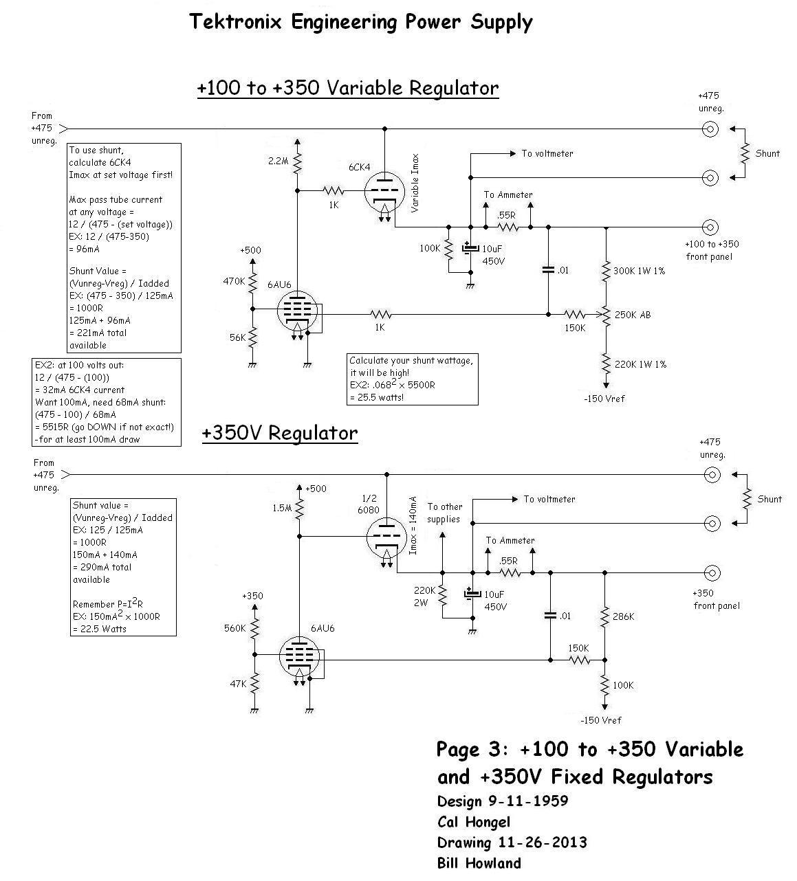
Here’s the third schematic page complete with shunt calculation data. There’s plenty more to come.
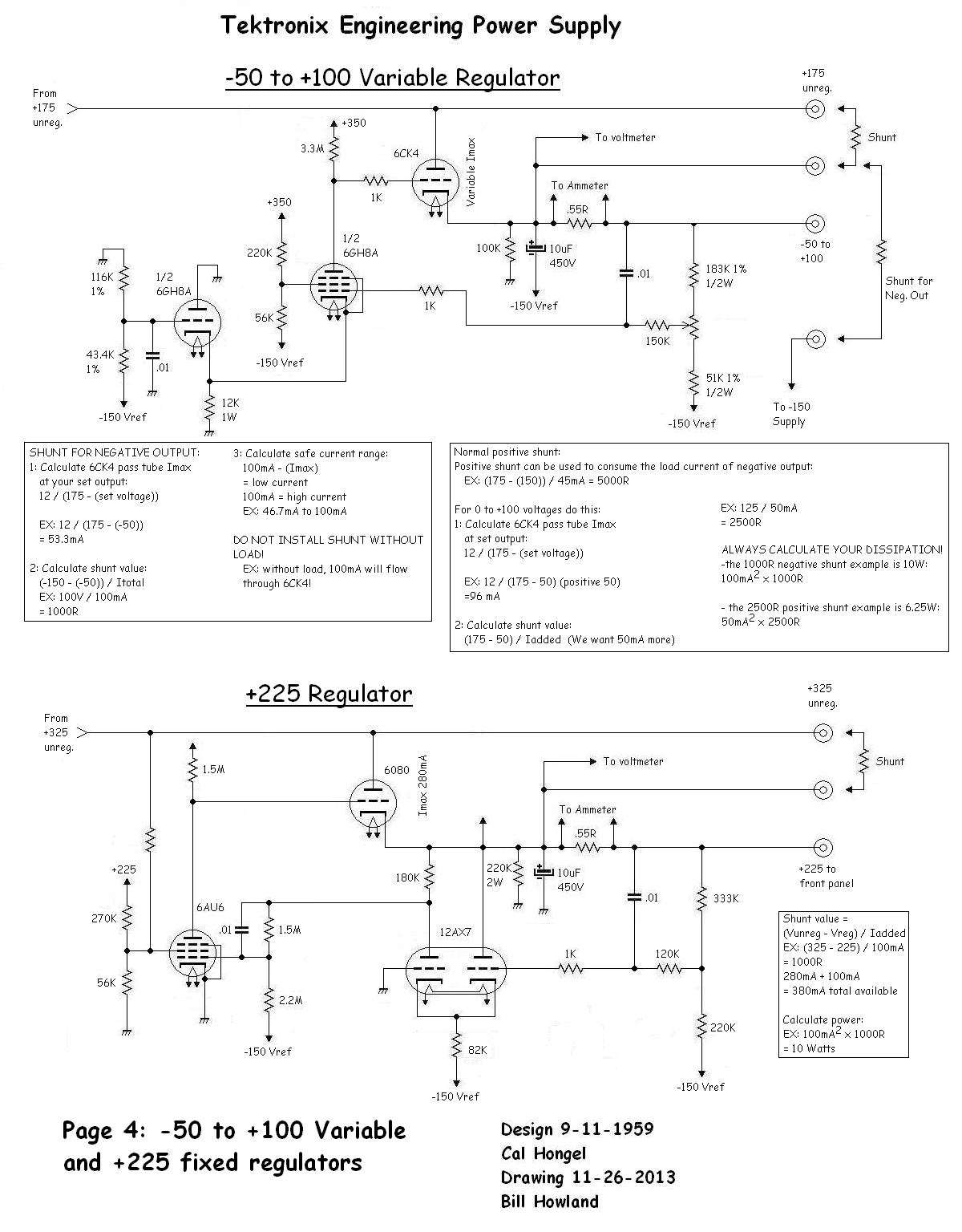
Here’s another page. The negative supply can be the most difficult to understand. You have to keep in mind that the reference point cannot be changed, so the shunt is merely a voltage divider that is using current flow to lower the voltage to the negative value as referred to ground.

The chassis for that looks like it’s made from the external power supply of a TEK 551 or 555 scope.
Very cool, and thank you for sharing.
I’ve never found a picture of something with these dimensions on TekWiki, but it is mostly stamped like a production chassis with a few mods. There are unused holes, etc. I’d bet each one of these is different in some way!
You’re right. I just looked and the 555 power supply is completely different inside.
And the housing looks much wider (looking form the top).
It seems unlikely though the stamped end panel isn’t from another standard product.
Maybe the Type 132 plug-in power supply.
The actual panel with the tubes and ‘lytics in your unit looks a lot like what’s in a 541/545 etc.
Sorry to keep bombing you with comments. 🙂
The chassis of your power supply… the missing tubes on the left side, V885 and V875 match the calibrator of the type 541A.
And the other tubes match the power supply. V609 for example is a 5651 in the 541A.